
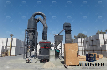
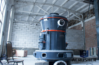
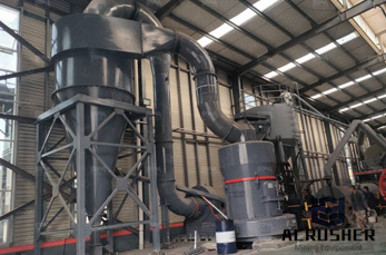
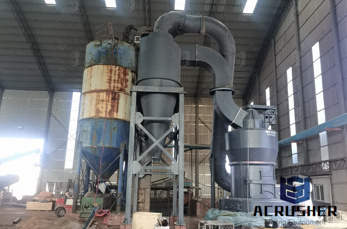
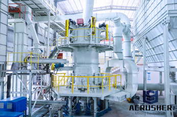
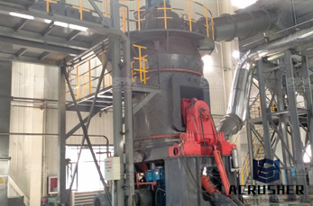
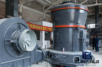
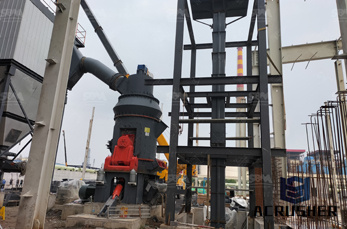
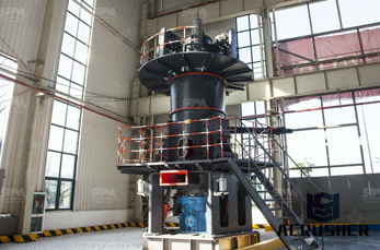
Wafer Back Grinding Process manufacturer Grasping strong production capability, advanced research strength and excellent service, Shanghai Wafer Back Grinding Process supplier create the value and bring values to all of customers.
 WhatsApp)
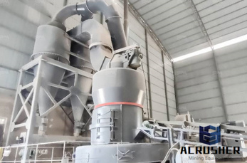
Back Grinding For Bare Device Patterned Wafers,SVM,Inc. Back grinding is a process that removes silicon from the back surface of a ... wafer back grinding process.
Figure 1. a) A backgrinding process leaves a characteristic scratch pattern on the back of the wafer. b) The back of the die from certain locations on the wafer have ...
Effects of back grinding process ... Wafer Reclaim and processing services including wafer grinding and thinning, wafer edge trimming, wafer dicing, ...
The present invention relates to a process for the backsurface grinding of wafers using films which have a support layer, which is known per se, and an adhesion ...
Semiconductor Wafer Edge Analysis/4 Stricter requirements in the wafer manufacturing process have made edge measurements important for both 200 mm and 300 mm wafers.
BackSide Wafer Grinding Quality Affecting BackEnd Assembly, back grinding process,ABSTRACT Die size and thickness of IC .
GDSI, Grinding and Dicing Services complete resource for Silicon Wafers Processing includes Probing, Bumping, Grinding, Polishing in San Jose, California.
Syagrus Systems thin wafer backgrinding and silicon wafer thinning services meets ... more about our Wafer Dicing Process. ... your next back grinding wafer ...
The TAIKO process is the name of a wafer back grinding process that uses a new grinding method developed by DISCO. This method is .
Plasma systems for wafer stress relief ... process containing no free ions or electrons that could potentially charge the surface of the wafer. The backgrinding ...
Introduction of Product Introduction of Wafer Surface Grinding Machine Model GCG300 Junichi Y amazaki Meeting the market requirements for silicon wafers .
This study investigates warping of silicon wafers in ultraprecision grindingbased backthinning process. By analyzing the interactions between the wafer and t
Semiconductor BackGrinding The silicon wafer on which the active elements are created is a thin circular disc, typically 150mm or 200mm in diameter.
Wafer backgrinding is a semiconductor device fabrication step during which wafer thickness is reduced to allow stacking and highdensity packaging of integrated ...
Wafer Backgrind is the process of grinding the backside of the wafer to the correct wafer thickness prior to assembly. It is also referred to as ''wafer ...
Back grinding is a process that removes silicon from the back surface of a wafer. Silicon Valley Microelectronics provides grinding on our own substrates or on ...
Effect of Wafer Back Grinding on the Mechanical Behavior of Multilayered Lowk for 3DStack Packaging ... generated during wafer back grinding process affect the
parallelism between the front and the back surface. Secondly, the grinding ... achieve this we need to understand thoroughly the process of semiconductor wafer grinding
Warping of silicon wafers subjected to backgrinding process ... grindingbased backthinning process is featured with a ... act on the wafer subjected to backgrinding,
Custom Silicon Wafer Back Grinding Services SVM. Back grinding is a process that removes silicon from the back surface of a wafer Silicon Valley Microelectronics ...
Wafer Pick And Place Service Grinding and Dicing This process allows you to extract particular die from a wafer and place them back on Wafer Grinding Polishing ...
Warping of silicon wafers subjected to backgrinding process. This study investigates warping of silicon wafers in ultraprecision grindingbased backthinning process.
Wafer Back Grinding Tapes AI Technology, Inc. Wafer Back Grinding Tapes Rework Process White Papers Wafers requiring grinding and .
back grinding process + crushergrinder. Wafer backgrinding + Wikipedia, the free encyclopedia Wafer backgrinding is a semiconductor device fabrication step during ...
WhatsApp)